Creatz3D has delivered 600 sets of 3D printed alumina lift pins to a global semiconductor foundry after the components passed full production qualification for chemical vapor deposition chambers. Using ceramic additive manufacturing technology from 3DCERAM SINTO, the Singapore-based company completed printing, debinding, sintering and post-processing in six weeks.
The companies say local production shortened supply lead times from months to weeks, helping the foundry maintain uninterrupted qualified production while reducing its dependence on overseas sourcing. The customer has not been named.
Small ceramic parts with demanding wafer-handling duties
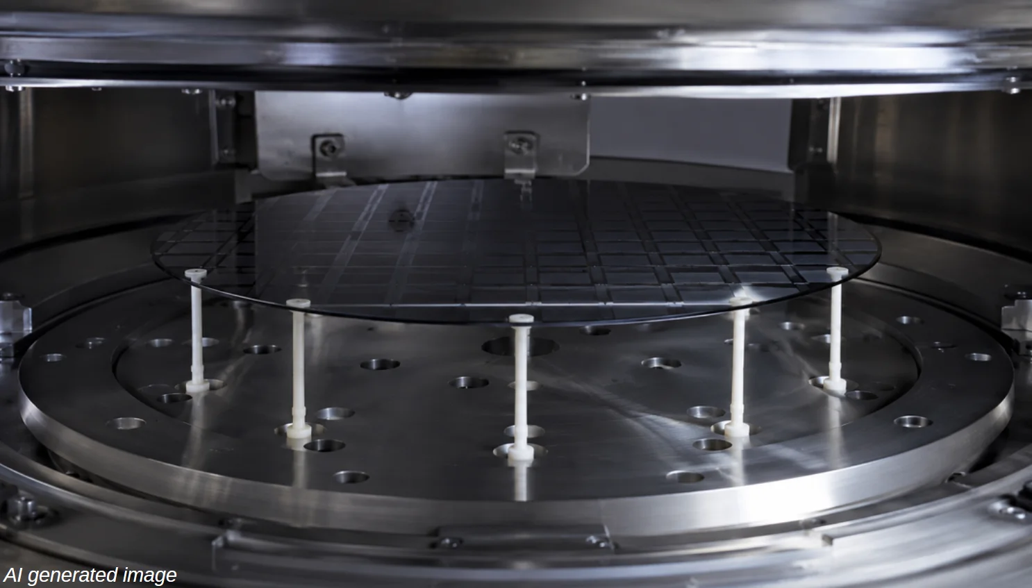
Lift pins support and precisely position silicon wafers inside semiconductor process chambers. They are used in chemical vapor deposition, physical vapor deposition and atomic layer deposition, commonly abbreviated as CVD, PVD and ALD.
High temperatures, vacuum conditions and exposure to plasma make dimensional stability, wear resistance and minimal particle generation important requirements. The pins must perform their handling role within those demanding environments.
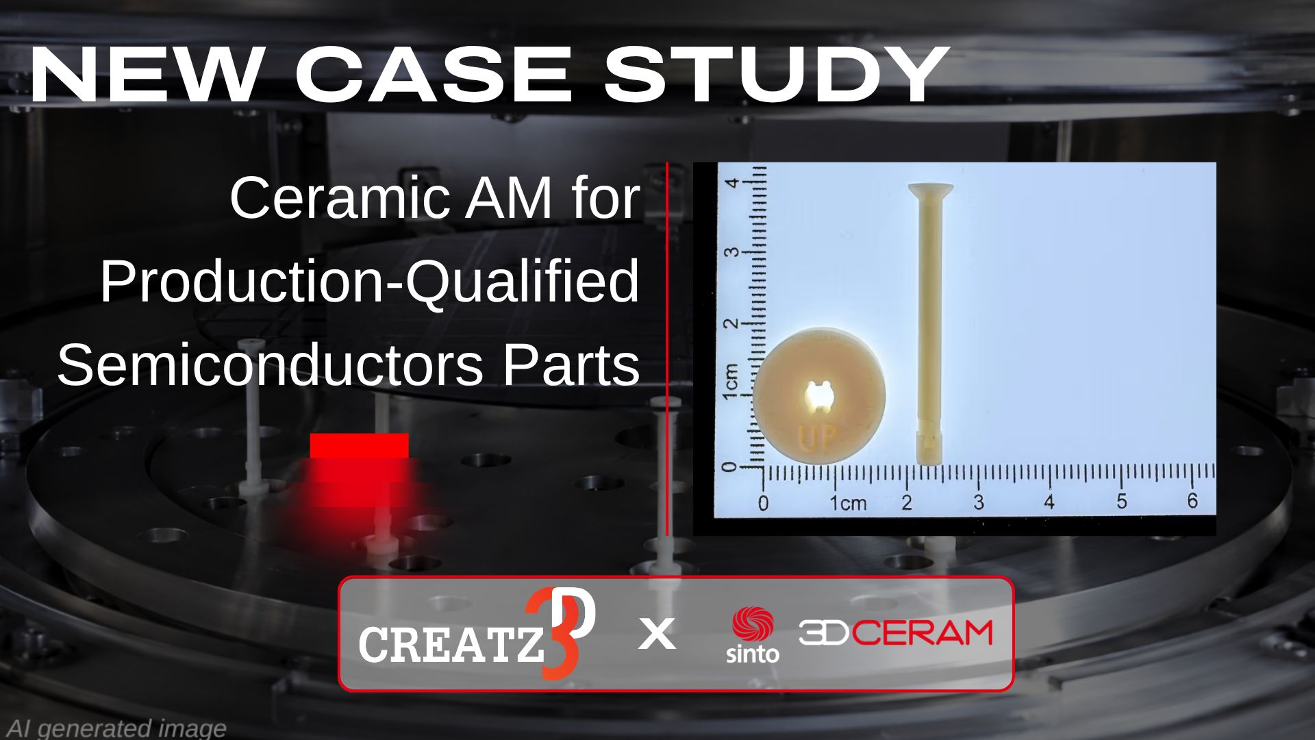
For this application, Creatz3D used alumina, Al₂O₃, selected for its mechanical strength, fracture toughness, wear resistance and electrical insulation properties. Each component combines a slender pin with a wider base:
- Pin diameter: approximately 6.5 mm.
- Pin height: approximately 40 mm.
- Base diameter: approximately 20 mm.
- Base height: approximately 4 mm.
Creatz3D manufactured the customized components to tight dimensional tolerances before taking them through the foundry’s qualification process. The delivery puts a concrete production quantity behind the project: 600 validated sets for semiconductor equipment use.
How top-down SLA fits the production process
3DCERAM SINTO attributes part of the result to its top-down stereolithography architecture. In this process, exposure takes place from above into a ceramic-filled resin. That arrangement avoids the peeling forces associated with separating printed layers from the transparent base surface in bottom-up systems.
The manufacturer says eliminating those forces improves process stability. It also cites support-free printing, the ability to produce large and dense components, and freedom to form complex internal geometries among the architecture’s benefits. Repeatability and homogeneous material properties after sintering are further claimed advantages.
Printing was only one stage of the lift pin production cycle. Debinding, sintering and finishing followed, taking the parts through the processing needed to achieve their final properties and dimensional tolerances. The reported six weeks covered that complete manufacturing sequence.
The partnership behind the work dates to 2016, when Creatz3D and 3DCERAM began collaborating on ceramic additive manufacturing in Singapore. Creatz3D’s work with functional technical ceramics includes semiconductor equipment applications in etching and CVD environments.
Regional production networks put qualification at the center
The lift pin project fits a broader approach pursued by 3DCERAM SINTO: pairing its machines with regional partners that can manufacture and qualify ceramic components close to industrial customers.
Lithoz uses a similar partner-based model through its Ceramic 3D Factory, a network of contract manufacturers producing parts for OEMs. Its applications include aluminum nitride cooling plates for semiconductor equipment. Lithoz has reported 40% growth in ceramic material revenue, driven by increasing production volumes across that network.
Material expansion is following the same emphasis on qualification. Sinto Advanced Ceramics added aluminum nitride and silicon nitride to its printing portfolio, with aluminum nitride offering electrical insulation alongside high thermal conductivity for semiconductor applications. Its qualification approach covers printing, debinding, sintering and quality assurance before materials are offered to industrial users.